Czochralski silicon wafers
Versatile substrates with controlled dopant and resistivity options.
 NIKUNJ'SNANOTECHRequest a quote ↗
Product catalogue
Browse core, special-dimension and engineered wafer categories—each available as a starting point for a focused technical quotation.
Request product pricing ↗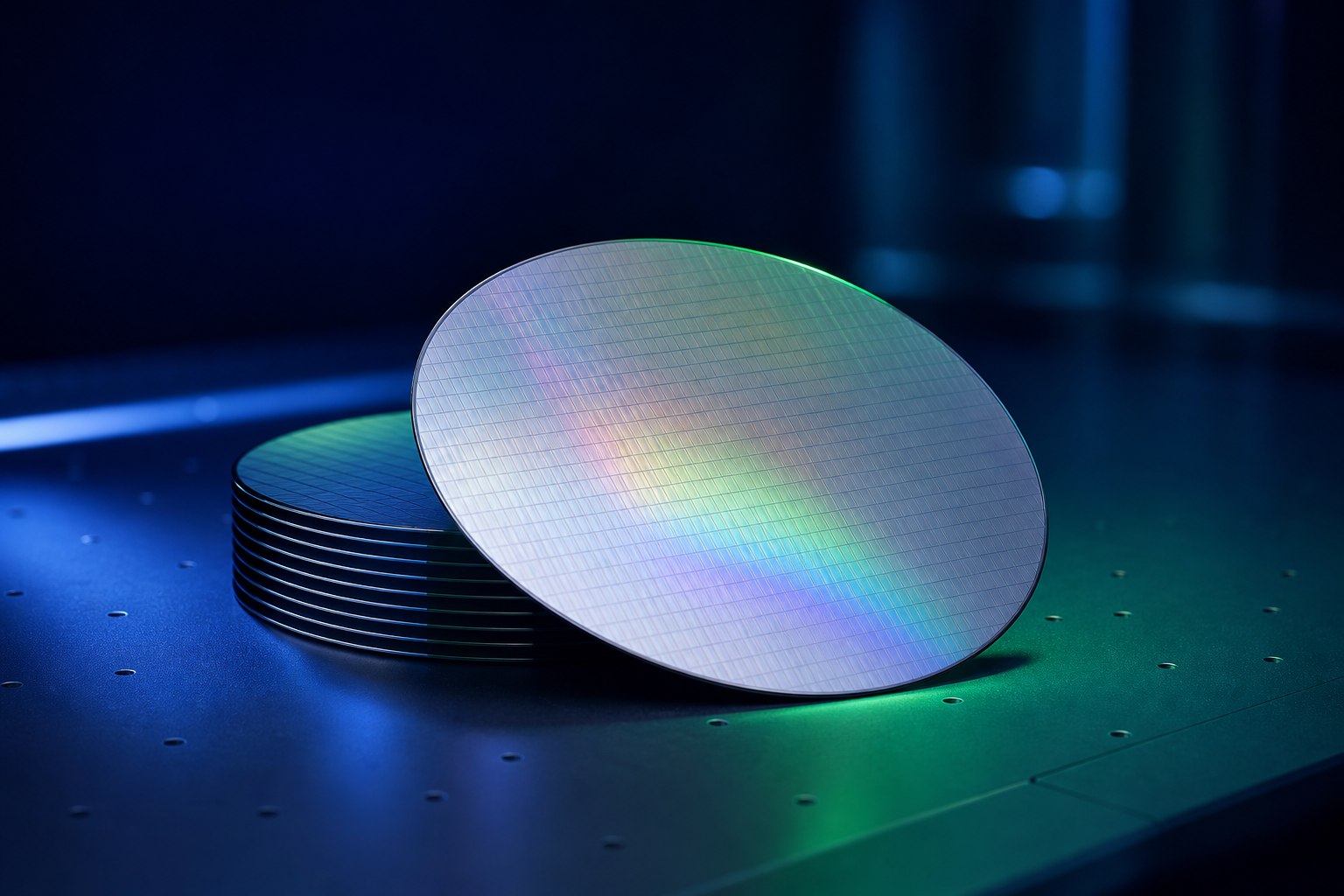
Portfolio
Foundational substrates for semiconductor fabrication and research.
Versatile substrates with controlled dopant and resistivity options.
High-purity, low-oxygen material for demanding electronic applications.
Engineered device and handle layers for MEMS, RF and photonics.
Precision glass substrates for microfluidics, packaging and optical systems.

Portfolio
Material formats aligned with development, testing and production needs.
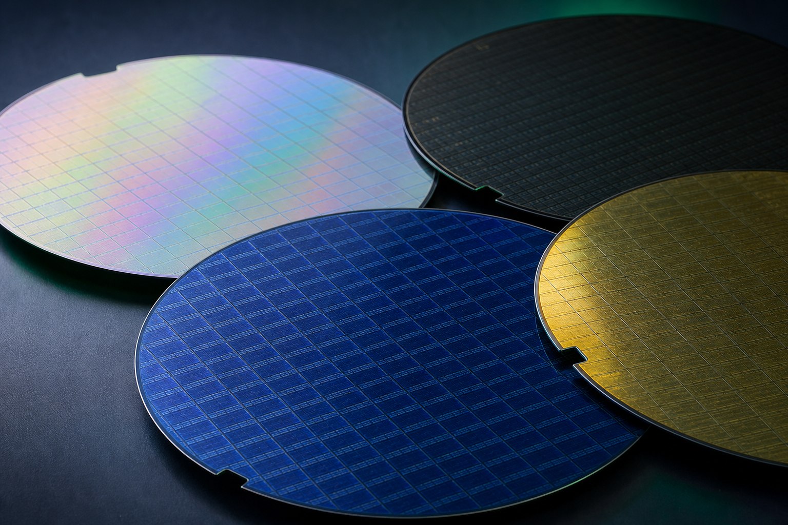
High-quality polished wafers for device production and critical processing.
Cost-effective process-monitoring and equipment-qualification substrates.
Restored substrates for non-device runs and process development.
Precision-cut pieces and dies prepared to specified dimensions.
Portfolio
Custom dimensions, surfaces and layers for specialized processes.
Precision-thinned substrates for compact and high-performance devices.
Robust substrates for specialty handling and mechanical applications.
Controlled SiO2 layers for insulation, masking and research.
LPCVD or PECVD SiN films tailored to process needs.
Engineered metal coatings for device and research applications.
Technical enquiry
Share your requirements and get a focused technical review from our team.